The Power
Amplifier
The design considerations
taken to arrive at the final design are detailed below .
Various options were considered
:-
A
pair of Single ended amplifiers with a splitter & combiner or "Push
pull " pair .
The next question of course is what type of
active device, Bipolar or FET
Given that a "Push pull
" style of amplifier should if the active devices have the same
electrical characterisics have a better performance , which means superior
suppression of "even " harmonics , this in turn means that filtering
requirements for remaining harmonics are also reduced .
The Amplifier circuit finally
chosen to give the required output power is a " Push - Pull " design
using a "Twin" package transistor ie one in which the two devices are
manufactured on the same die so that their characteristics are as near a match
as possible .
Then supply voltage for the
chosen device , obviously the higher the supply voltage ( within reason ) the
easier the matching of the device's impedance to the system impedance ( 50 Ohms
) so the choice between 12 V, 28 V & 50 V was settled in favour of the 50
volt devices , this does however reduce the choice of device available . There
were three types chosen MRF151G from Motorola ( On Semi ) BLF278 from Philips (
NXP ) and the D5028 from Semelab , in the end the D5028UK was chosen due mainly
to the lead time to obtain the device for another student's projects .
The amplifier was designed to
have a flat frequency response across the whole 2 meter amateur band by using
transmission lines for the matching networks rather than discrete components
this also has the advantage of increasing the reproducabilty of the design for
other constructors , the choice of PCB material dictates the size of the
completed amplifier as well as the size of the heatsink .
The heatsink size also
dictates the size of cabinet chosen for the completed design so that it could
be fitted in to the case , a small flow of air would be passed over the
heatsink using standard fans as used in computer power supplies, these can be
run at lower voltages to reduce the noise generated under normal operating
conditions if the heatsink temperature exceeds the required " Ambient
temperature " as used in the calculations then the air flow can be greatly
increased by using the fans at their rated supply .
The amplifier is biased into class AB as it is intended for
both SSB & FM modes of operation this means that it will be at best 50%
efficient so for 200 Watts output from the unit there will be at least 200
Watts of heat to be dissipated by the heatsink when in the input is an FM
signal, the mean value of an SSB signal being somewhat lower means that it will
run cooler . Due to the amplifier being intended to run at high power for
continuous operation the use of " FR4 " pcb material was eventually
discounted due to the transmission lines in the matching networks being too
thin to efficiently dissipate the heat due to the circulating currents , the
prototype amplifier used FR4 with " Smoky " results when the Drain
output matching network caught fire due to the inability to handle the
circulating currents ( It may also have been due to the use of a single
capacitor in this place ) so the final version of the amplifier used a "
Duroid " RT5870 - 060 - C1/C1 with 1oz copper " ( Although 2oz /
square inch would have been better ) , the area under the output transmission
lines being smeared with a thin film of heatsink paste to assist in the removal
of the heat . The construction of the
amplifier module case was from aluminium plate & bar stock from a local DIY
shop ,with only a small amount of machining done to attach the parts to the
heatsink the usual precautions are taken for any RF power module all
connections to it are either using coaxial connectors or feedthrough capacitors
preferably of the " Pi " type internal construction so that any RF
signals superimposed on supply or control / sensing wiring will be decoupled
from either direction all supplies & signal paths on the amplifier pcb are
also liberally filtered to minimise any stray resonances within the module's
case .The choice of capacitor for the RF matching circuits was down to either
the " ATC 100B " series of capacitor from " American Technical
Ceramics or the equivalent " CHB " series made by " TEMEX "
again due to the magnitudes of the currents involved " multiple parts were
used in parallel to ensure the reliability of the unit over time by minimising
the stresses induced in the devices , it's is possible to " Fuse "
the internal plates of the capacitor away from the end terminations due to
" I2R " losses within the device , the main tuning points for the
matching circuit had a small trimmer capacitor with PTFE dielectric to give
about 5% adjustment to optimise the match of both the input & output
networks to system impedance ( 50R ).When first modelled it became obvious that
the transmission lines used in the matching circuits would be too long as
" Linear " circuits so the lines were redesigned into a series of
" Hairpin Loops " with short sections of transmission line parallel
to each other only where the chip capacitors needed to be ( see the layout /
circuit for more detail ) the width of the transmission line was chosen to be
near to system impedance for the mounting of the input & output "
Baluns " but was then remodelled using the width of the acitve device to
give a better heat dissipation / enable more capacitors in parallel to be used
this impedance was 43 R ( 6 mm wide track ).The amplifier's heatsink
temperature is measured using an LM35CZ temperature sensor in a small pocket
filled with a small amount of heatsink paste adjacent to the transistor this
produces a voltage output of 10mV / deg C for the control board .
The amplifier as modelled
using " Microwave Office " below
PCB Layout for the amplifier
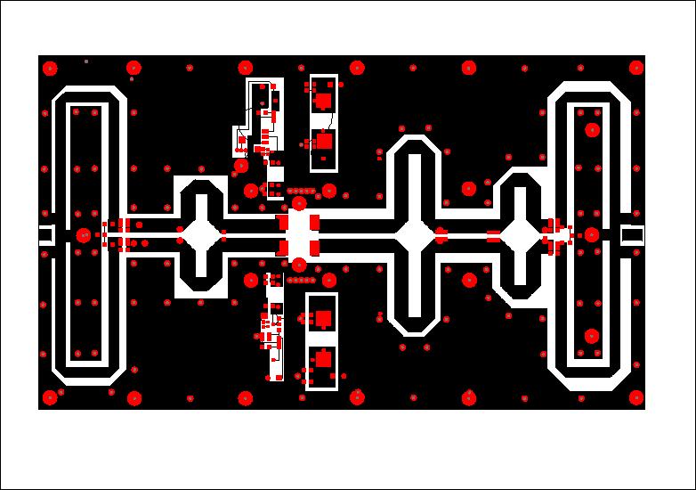
Mirrored Artwork for the amplifier
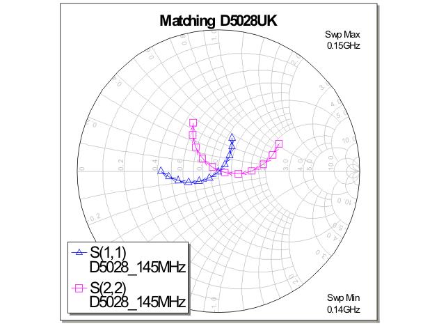
Screen shot of Input & Output Matching on
a Smith Chart as modelled using " Microwave Office " below
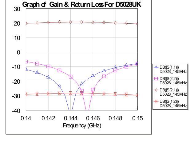
Screen shot of Amplifier Gain &
Return loss as modelled using " Microwave Office " below
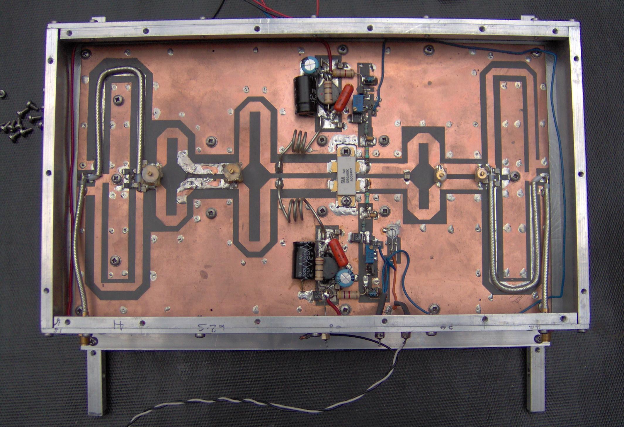
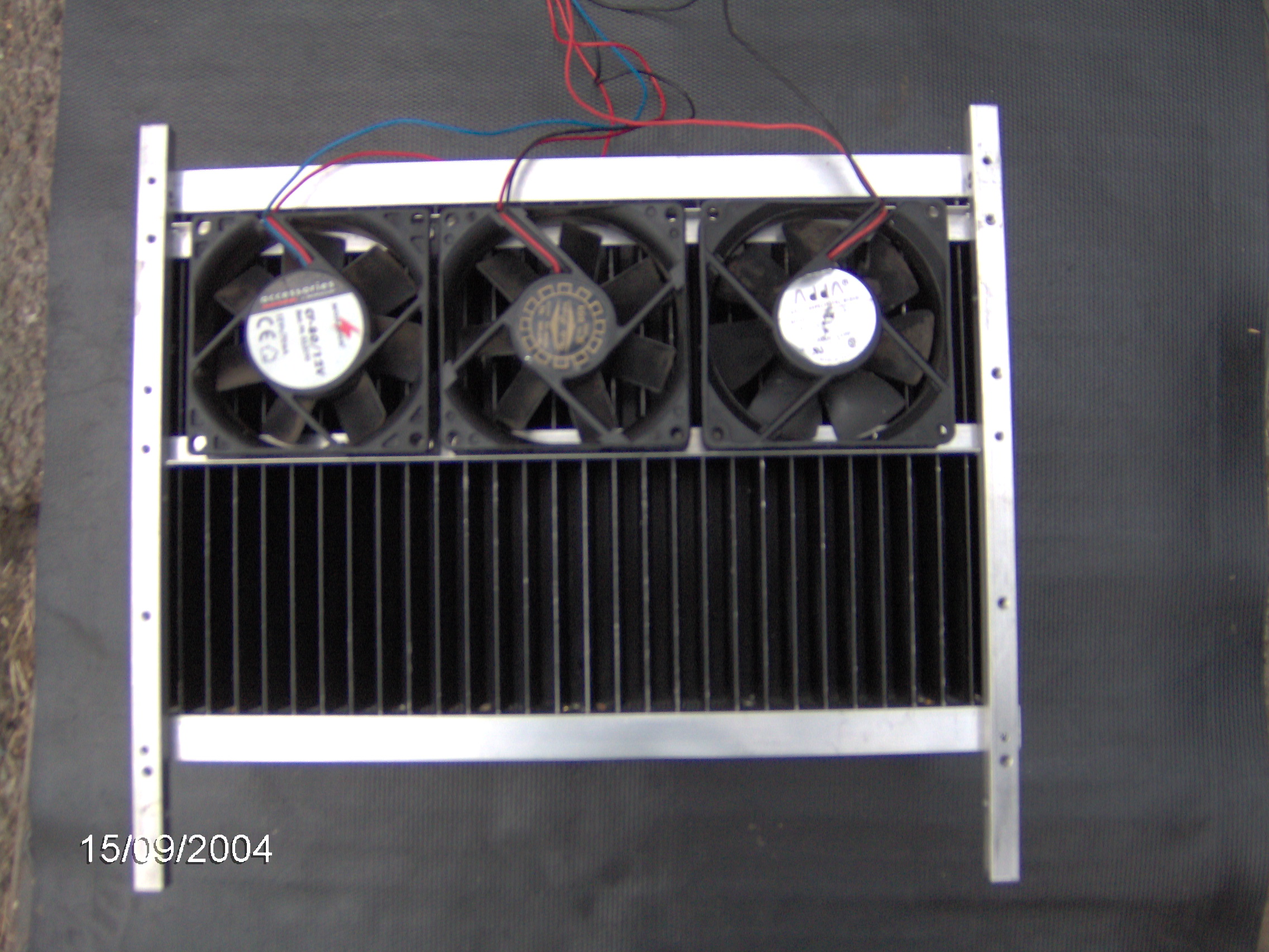
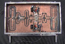
The amplifier module during
testing as built below
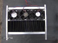
Picture of completed amplifier
module with fans fitted during testing
The parts listing for the complete amplifier
module will appear shortly
Back To Table Top 200
Watt 145MHz Amplifier
This page last updated 10th Nov 2009